Copyright 2008 Brian Brzezicki, all rights reserved. Feel free to link to this or use the information within, but please give credit where credit is due.
9/26/2008 write up version 1.22 - Added info on how to do this with a -03 or -04 board in the Questions and Answers section.
9/26/2008 write up version 1.21 - Added info on how to do the hack without cutting the PCB wires in the Questions and Answers section, and also uploaded the tubes ROMS version for 256k and 512k.
9/25/2008 write up version 1.2 - These hacks will not work as is with version -03 or -04 boards or any board that's using 5 32kbit ROMs rather than 10 16kbit ROMs
9/25/2008 write up version 1.1 - added 512kbit tempest and tubes ROM
9/24/2008 write up version 1.0
This is a wrete up of some hacks that you can do to a tempest board. Please note the following.
Disclaimers
- I'm certain I'm not the first person to do these hacks or write them up, and I'm not claiming to be the first. In fact... I know for a fact that others have done at least one of these before me. However when I was looking for information on how to do these hacks in Sept 2008... I could not find them...anywhere... after searching for a few hours I decided to try to figure out what was needed myself. I am writing them out to help out others who are looking for the steps necessary. I will also document not only "what steps to take" but "why" so anyone else who'd like to learn a bit about CPU/memory architecture or board hacks will have some reference.
- I beleive these hacks will work, either from trying them myself or just simpe theory... but I take no responsbility if you try these and it messes up your machine or causes any type of damage to your property or yourself. So if you try these, understand that you do them at your own risk. do not sue me or complain if your try them and your board breaks or it causes some type of damage to you or your property.. in fact I wouldn't recommend hacking any board unless you have a reason to (like trying to fix a board that might be damaged in the ROM area, or if you don't have working 2516 ROMs to replace broken ones with)
- These should work on unhacked version -01 or -02 CPU boards.
- These WILL NOT work as is on version -03 or -04 boards or any board hacked to use 2532 chips (ie if you only have 5 game ROMS on your original board.. this will NOT work for you.) There are additional isntructions in the Questions and Answers section that you can take that "should" make it work on these later boards.
The following hacks are described
- Hack 1: Replace 10 game ROM chips with a single 256Kbit chip (27256)
- Hack 2: Replace 10 game ROM chips with a single 512Kbit chip (27512) (these are easier to find and seem to be cheaper than the 27256)
- Hack 3: Repalce 10 game ROM chips with a single 512Kbit chip (27512) and have both tempest and tempest tubes playable selectible via a switch.
Please note, for the steps that require cutting the PCB board.. you CAN do it without cutting the board, but you need to buy an extra IC socket... see the explainations section at the bottom for instructions on how to do this.
Hack 1: Replace 10 game ROM chips with a single 256Kbit chip (27256)
Note: I've tested this on my own board (2 of them) both version -01 and -02 PCB boards... works fine... still do this at your own risk.
- remove the 10 game ROM chips (D1, E1, F1, H1, J1, K1, L/M1, M/N1, P1, R1) from the tempest ROM sockets. (these are in a row at the edge of the gameboard close to the interboard connector)
- Leave the Video ROMS (np3, r3) intact, do not remove them.
- Desolder the chip socket at ROM slot D1, we will need to cut some traces underneath the socket.
- In ROM chip slot D1, on the PCB board cut the thin trace going from pin 20 on the top side of the board)
This is the "Output Enable" pin. The new chip will have an output enable pin in the same location, but we'll need to tie it to the the inverted output of address line 15. (the reason we cannot use the original trace is because since there were 10 chips, the output enable on ROM slot D1 will only be correctly set 1/10 of the time.
- There is a trace (on the underside of the board) from pin 21 to 24 in ROM slot 0, Cut this trace, on the 2516 chip, this was Vpp which was tied to put 24 (Vcc) but the new chip in there this pin will be address line 11.
- There is a trace connecting pin 24 to +5V (on the top side (parts side)) of the PCB board, cut this trace, as in the new chip the pin in this location is actually Address Bus bit 13
- solder back the socket... or better solder in a new 24 pin IC socket.
- Now we have to program a new ROM, get a 256kbit ROM chip. program the chip starting at address 1000 (hex) program it so the following original ROM chips are concatenated right after each other, ROM D1, ROM E1, ROM F1, ROM H1, ROM J1, ROM K1, ROM L/M1, ROM M/N1, ROM P1, ROM R1, and then ROM L/M1 (again), ROM M/N1 (agaim), ROM P1 (again), ROM R1 (again)
after all these are done your chip should be filled up, you can also use the tempest tubs code if you prefer. Or simply use the concatenated ROM image file located here (tempest V3) or here (tubes)
if you use either of these pre-made ROM images, DO NOT start at address 1000 (hex) the image is already offset to start at location 1000 (hex)
(If your wondering why ROM 5,6,7 and 8 are repeated see
http://www.kfu.com/~nsayer/games/tempest.html read the "Memory map" and the "Microprocessor and CPU support systems" section)
- put the new 256Kbit ROM socket in the slot D1, configure it so that the back of the chip (pins 14, and 15) are where the back of the original chip was (pins 12, and 13), the first 4 pins will be haning off the front of the socket.
- Gently bend up pins 1,2, 27, and 28 (pins relative to the NEW chip). so they are parallel to the PCB board.
- solder a thin wire from pin 1 on the new 256K chip... run this to +5V
- solder a thin wire from pin 28 to +5V
- solder a thin wire from pin 2 to address line 12 on the memory address bus, this can be found at pin 3 on LS244 in slot A/B1
- solder a thin wire from pin 27 to address line 14, this can be found at pin 3 on LS139 at slot B3
- solder a thin wire from pin 26 to address line 13 this can be found at pin 2 in LS139 in slot B3
- solder a thin wire from pin 23 to address line 11, this can be found at ping 18 on LS244 at slot A/B1
- solder a thin wire from PIN 22 to logical NOT address line 15... this can be found at pin 4 on LS04 in slot A6 this is the Output Enable pin and should be set LOW (that is enableing output) whenever the CPU address bus has a 1 in bit 15 of the address line....
actually forget soldering it to PIN 4 on LS04..you can take a shortcut and just tie this to ground... the out output buffer chip will end up disabling the ROM from the address bus unless if the CPU has not requested an address in that range, so the ROM can actually always be active without harm.
That's it
Hack 2:Replace 10 game ROM chips with a single 512bit chip (27512)
Note, I have NOT done this yet to my boards... but the theory is sound.
- Do all the steps above, but when programing, use a 27512 EPROM rather than a 27256. You also need to start the ROM at address 9000 (hex) for the 27512 rather than address 1000 (hex)... or start programming at location 0000 (hex) and use the image file here (tempest v3) or here (tubes) which is already offset to location 9000 (hex). The reason you can do this is because pin 1 on the 27512 is address line 15, in the previous hack we wire pin 1 to +5V, so we must shift the address start to the same as 1000 (hex) but with address bit 15 set, 1000 (hex) becomes 9000 (hex) (interestingly that's the actual memory location of the ROM code in the tempest CPUs 64k address space)
Hack 3: Replace the 10 game ROM chips with a single 512bit chip (27512) and allow either tempest regular or tempest tubes selectible via a switch.
Note, I have NOT done this yet to my boards... but the theory is sound.
update 06/27/2016 - I have been emailed by someone who confirmed they did this on the board and it worked.
- Follow the instructions for hack #1, but skip step #11, and skip step #8.
- on pin #1 of the 512Kbit ROM, wire in a 10K resistor between pin #1 and ground, also wire pin #1 to one terminal (we'll call it terminal A) of a continous switch (one that is not a momentary switch... for example a DIP switch is great) and the other terminal (terimnal B) of the switch to +5V.
- Program the ROMs the PROMs the same in step #8 from hack #1 (except use a 27512 obviously), however then starting at address 9000(hex) also program in the tempest tubes full ROM set. when the switch is open, address line 15 will be low and the regular tempest game will be mapped into the games address space, when the switch is set address line 15 will be high and causing the tempest tubes to be mapped into the CPU's address space. Alternately set your eprom programmer to start at address 0000 (hex) and use the ROM image here
If you want to play tubes, you should just have to turn the switch on.
Questions and Answers:
Q. With the 25256, Why do you have to start programming at address 1000 rather than start at 9000
A. because with a 256K chip the highest addressable number would be 7FFF!. if you moved to a 512K chip then you could start programming at 9000 instead.
however since the ROM range is only selected if the CPU has the high address bit set, we can just shift the address range down 1 bit, (which makes it 1000) and start programming there, then tie the high address bit from the CPU (actually the complement of that.. and tie it to the chips output enable and get away with using a smaller chip.
why don't we just start programming at address 0 on the big chip? at first this seems logic, but if we do that we have to remember that in the real memory map the ROM code does NOT start at 0, it starts at 9000, so we have to build in an extra logic circuit to calculate the chips real addresses into the relative addresses on the ROM, it's just easier to move the starting address range on the ROM so that it is no longer relative , (well relative, ignoring the high bit which we can o since the ROM isn't actually addressable in that range (32K-64) and that bit will actually tie into enableing this chips output.
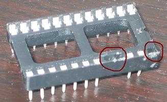
Q. How do I do these hacks without cutting the PCB board.
A. Instead of removing the original socket and cutting the PCB boards, you can leave the initial socket in place, buy another 24 pin socket. (Digi-key.com part #3M5467-ND). Then rather than cutting the pcb traces from the IC pins, simple remove the metal connectors for those associated pins from the new IC socket. Then plug the new IC socket, into the original IC socket on the board, and plug your ROM chip into your new modified socket! This way you can do the hacks and if they don't work or you want to revert back to your original setup there's no permanent damage... simply undersolder the wires you added and also remove the extra IC socket and put the ROM back into the original socket! For example for hack #1 and #2 you'd skip steps, 3,4,5,6,7 and instead you'd get a new IC socket, remove the metal connectors on the IC socket for pin #20,#21,#24
Q. Can I do this on a -03 or -04 version board that has 5 32Kbit chips?
A. You should be able to do this.. however you'll need to do an additional 2 steps.
- Cut the PCB trace from the pin 18 (relative to the original 24 pin ROM)
- Wire this pin you just cut to ground, please note... when you go to wire it you'll be wiring it up to the new 28 pin ROM which that same pin will now be located at pin #20!... (or just count the 6th pin from the back... that way you don't have to worry about pin numbering which changes when you put the new chip in since the the new chip is bigger and numbering starts from the top left!)
References used:
- Tempest PCB board drawings/schematics
- Nicholas Sayer's Tempest Detailed theory of operation.
- MAME source code tempest driver (tempest.c)
- Tempest Tubes/Original Tubes Hack (idea of using a switch to remap the address space into different segements of a larger ROM)