Galaxian step by step troubleshooting Guide (Midway board #A082-91352-C000 #A080-91352-C000)

Copyright Brian Brzezicki 2014
This is a work in progress
Version 1.3 - last update 7/12/2014 Now with hidable windows!

Troubleshooting steps - start here

Troubleshooting Steps - Start here

  1. Check for a valid clock signal, use a logic probe or oscilliscope to ensure a signal on pin #6 of the Z80 @ B7. Output should be a steady signal at 3Mhz.

  2. Turn game off, using a logic probe or oscilliscope measure the !reset pin on the Z80 CPU @B7 (#pin #26).
    • Signal should start HIGH then briefly transition to LOW after power is applied, the return back and stay HIGH for the rest of the time.
    • If the signal never goes low or STAYS low permanently then your reset circuit is broken, skip to the section troubleshooting the reset circuitry.
    • If signal transistions back and forth from high to low, then the watchdog is resetting the game properly and the game is broken elsewhere.. continue with the next troubleshooting step.

  3. If you have a Fluke 9010A validate the game ROMS.

  4. If you have a Fluke 9010A validate the various RAM circuits.
  • If you have gotten this far, the game should be booting up and playing (perhaps blind) but the main CPU/memory/ROM circuits are good. The game might have graphic or sound glitches but should be working for the most part.
  • Testing the ROM circuitry

    Testing ROM circuitry

    Use your Fluke 9010A and a logic probe or oscilliscope for these tests.

    Theory: The ROM circuits are pretty straight forward.

    • There are the 5 GAME ROM chips usuauly on a daughterboard.
    • There are 2 address buffers (74LS365 or 74LS367) @ D7 and E7 that are essential for the operation of the game.
    • There is a 74LS139 @ E8 that controls address selection (chip enable) for ROMs, this is the entire ROM address decoding circiut on the mainboard.
    • There is a 74LS42 on the daughter board that controls address selection (chip enable) for the ROMs on the daughterboard.
    • That's it... there's nothign else in the ROM circuitry!

    These tests below will systematically test the operation of the ROM address decode chips.

    • do a ROM test against ALL your ROMs first.
    • Use TABLE A below to find the first available address in the ROM range that's NOT working, as well as the address select pins that control your ROM range
    • Use the Fluke to READ the first address in your ROM range, put it in looping mode.
      • Is the Fluke output steady? if so continue, if it's fluxuating.. you have a problem of somethign else talking at the same times as the ROM. This is difficuilt to find, I cannot provide step by step instructions on that.
      • If the output is NOT fluxuating, are the select pins in the table below continually tranisitioning from high to LOW? If not replace the chip who's pin is not fluxuating (E8 or 74LS42 on the ROM daughterboard).
      • If you replace E8 and it still does not transition, then replace the Address buffer (74LS365 or 74LS367) at D7 and E7.
      • If the chips selects are transistioning, but your signatures is still bad, consider swapping another chip that tested OK, into the "bad" ROM position, and seeing if a ROM test on the ROM range in question matches the signatures of the known good chip. if it DOES, then replace the bad ROM.
    Testing the work RAM
    Testing video RAM

    Troubleshooting the Video RAM circuits

    1. First ensure you have tested and working work ram, using the work RAM troubleshooting steps
    2. Do a Fluke RAM long tests on range 0x5000 - 0x53FF
        Do you get ANY Errors?
        • NO - Video RAM is OK!

        • YES -
            Did you get a PATT error
            • ??? PLACEHOLDER ???

            Did you get a DCD error?
            • If YES - Replace the 2114s RAMs @ F3, H3

            Did you get a BTS error
            • If YES - Perform a RAM LONG test on address range 0x5800 - 0x58FF
                Did you get ANY error?
                • No - Replace the 2101s @ F4 and F5
                Did you get a BTS error?
                • No - Replace the 2101s @ F4 and F5
                • YES
                    Is the error BTS error FF?
                    • NO - Replace the VRAM address buffer (74LS245) @ B9
                    • YES - Verify the VRAM address selection circuitry (NEED TO ADD)

            Did you get some other error?
            • I'm not aware of any other Fluke memory errors! If so this troubleshooting guide cannot help you
    Testing object RAM

    Troubleshooting the Object RAM circuits

    1. First ensure you have tested
    2. Do a Fluke RAM long tests on range 0x5800 - 0x58FF
        Do you get ANY Errors?
        • NO - Video RAM is OK!

        • YES -
            Did you get a PATT error
            • Replace the 2101 @ F4, and F5

            Did you get a DCD error?
            • Replace the 2101 @ F4, and F5

            Did you get a BTS error
          • YES
            • If the error a BTS 0X error (X=any number) - Replace the next items one at a time testing after each replacement
              • 2101 RAM @ F4
              • 74LS367 @ M5
            • If the error a BTS X0 error (X=any number) - Replace the next items one at t time testing after each replacement
              • 2101 RAM @ F5
              • 74LS367 @ L5
              • 74LS367 @ M4
            • If the error a BTS FF error (X=any number) - Validate Object RAM address decoding - NEED TO ADD THIS

        Did you get some other error?
        • I'm not aware of any other Fluke memory errors! If so this troubleshooting guide cannot help you
    Testing the reset circuit
    Testing the clock circuit
    Tables

    Tables

    Table A
    Galaxian Midway Set 1 (galaxianm) Memory/Fluke 9010a information
    Memory RangeFluke 9010a SignatureROM locationROM Selection Pins
    0x0000 - 0x07FFFFDE7UE8 pin #4
    E8 pin #12
    74LS42 pin #1 on ROM daughterboard
    0x0800 - 0x0FFF40557VE8 pin #4
    E8 pin #12
    74LS42 pin #1 on ROM daughterboard
    0x1000 - 0x17FFFCD27WE8 pin #4
    E8 pin #12
    74LS42 pin #1 on ROM daughterboard
    0x1800 - 0x1FFF317B7YE8 pin #4
    E8 pin #12
    74LS42 pin #1 on ROM daughterboard
    0x2000 - 0x27FFEC3A7ZE8 pin #4
    E8 pin #11
    TABLE B
    Galaxian Midway Set 1 (galaxianm) Memory/Fluke 9010a information
    for the rom bypass method
    Memory RangeFluke 9010a SignatureROM locationROM Selection Pins
    0x0000 - 0x1FFF7FE8 pin #4
    E8 pin #12
    0x2000 - 0x27FFEC3A7LE8 pin #4
    E8 pin #11

    TABLE C
    RAM information (Courtesy of MAME)
    Memory RangeTypeMemory LocationNotesAddress Select Read PinsAddress Select Write PinsMain Data BufferSecondary Data buffers
    0x4000 - 0x43FF21147P (low 4 bits), 7N (high 4 bits)Work RAMH8 pin #15
    H2 pin #6
    M8 pin #15
    H2 pin #6
    NoneNone
    0x5000 - 0x53FF21143H (low 4 bits), 3F (high 4 bits)Video (tile) RAMH8 pin #13
    E8 pin #5
    M8 pin #15
    E8 pin #5
    B9 (74LS245)J5 (74LS245)
    0x5800 - 0x58FF2101F4 (low 4 bits), F5 (high 4 bits)Sprite RAMH8 pin #12
    E8 pin #5
    M8 pin #12
    E8 pin #5
    B9 (74LS245)J5 (74LS245)
    H5 (74LS367)
    L5 (74LS367)
    4M (74LS367)
    H5 (74LS367)

      Notes:
    1. Work RAM 0x4000 and ROMs (0x0000 - 0x27FF) are directly on the DATA BUS, there is no buffer between them.
    2. With a Fluke 9010A if you test 0x5000-0x53FF and 0x5800 - 0x58FF. If you get an error on one range check the other range for the SAME error. if it exist, more than likel your RAMs not bad, but you have a problem with the shared IO/RAM buffer 9B (74LS245), though some boards don't use 9B, instead use two chips 8F and 8H (8216) the 74LS245 and 8216 are both bi directional buffers.

    Sound

    in test mode you can jumper +5V to the following pins of 9L to get the respective sound
    Pin @ 9LSound
    4Rack Oscillating Sound 1
    5Rack Oscillating Sound 2
    6Rack Oscillating Sound 1
    7Fire
    10Explosion

    Sync Circuits

    here is a gem from the midway galaxian troubleshooting part 2 guide.
    You can check the sync circuits WITHOUT an o-scope by applying the output of the sync circuit to draw directly to the red, green or blue gun!

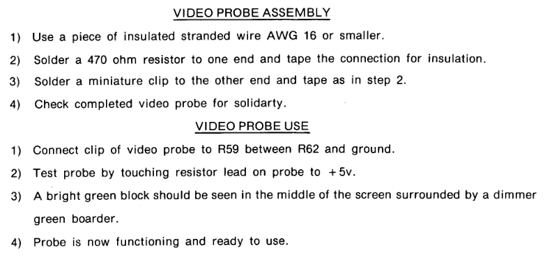
    First make a video probe using the instructions on page 3 of the guide

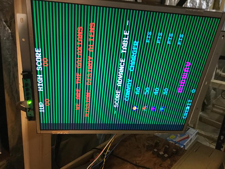
    Then leaving the one end connected to R59 between R62 and ground, test horizontal sync circuit at 3A, and 4A

    1. Touch the probe tip to pin #14 of 3A
    2. Touch the probe tip to pin #13 of 3A
    3. Touch the probe tip to pin #12 of 3A
    4. Touch the probe tip to pin #11 of 3A
    5. Touch the probe tip to pin #14 of 4A
    6. Touch the probe tip to pin #13 of 4A
    7. Touch the probe tip to pin #12 of 4A
    8. Touch the probe tip to pin #11 of 4A
    At as move from step 1 to 8 you'll noticed the green lines double in width on a working system The image below shows pin #14 @ 3A

    Now test the verticl sync circuits at 5A and 6A

    1. Touch the probe tip to pin #14 of 5A
    2. Touch the probe tip to pin #13 of 5A
    3. Touch the probe tip to pin #12 of 5A
    4. Touch the probe tip to pin #11 of 5A
    5. Touch the probe tip to pin #14 of 6A
    6. Touch the probe tip to pin #13 of 6A
    7. Touch the probe tip to pin #12 of 6A
    8. Touch the probe tip to pin #11 of 6A
    The same thing will occur this time starting with thin vertical lines that double in thickness from step 1 to 8
    Other references and sources of information